Author Affiliations
Abstract
Key Laboratory of Bio-Inspired Smart Interfacial Science and Technology of Ministry of Education, School of Chemistry, Beihang University, Beijing 100191, People’s Republic of China
Materials exhibiting high-performance electromagnetic wave absorption have garnered considerable scientific and technological attention, yet encounter significant challenges. Developing new materials and innovative structural design concepts is crucial for expanding the application field of electromagnetic wave absorption. Particularly, hierarchical structure engineering has emerged as a promising approach to enhance the physical and chemical properties of materials, providing immense potential for creating versatile electromagnetic wave absorption materials. Herein, an exceptional multi-dimensional hierarchical structure was meticulously devised, unleashing the full microwave attenuation capabilities through in situ growth, self-reduction, and multi-heterogeneous interface integration. The hierarchical structure features a three-dimensional carbon framework, where magnetic nanoparticles grow in situ on the carbon skeleton, creating a necklace-like structure. Furthermore, magnetic nanosheets assemble within this framework. Enhanced impedance matching was achieved by precisely adjusting component proportions, and intelligent integration of diverse interfaces bolstered dielectric polarization. The obtain Fe3O4-Fe nanoparticles/carbon nanofibers/Al-Fe3O4-Fe nanosheets composites demonstrated outstanding performance with a minimum reflection loss (RLmin) value of - 59.3 dB and an effective absorption bandwidth (RL ≤ - 10 dB) extending up to 5.6 GHz at 2.2 mm. These notable accomplishments offer fresh insights into the precision design of high-efficient electromagnetic wave absorption materials.
Nano-Micro Letters
2024, 16(1): 174
Author Affiliations
Abstract
1 Department of Electronic and Computer Engineering, The Hong Kong University of Science and Technology, Clear Water Bay, Kowloon, Hong Kong, China
2 e-mail: wluoag@connect.ust.hk
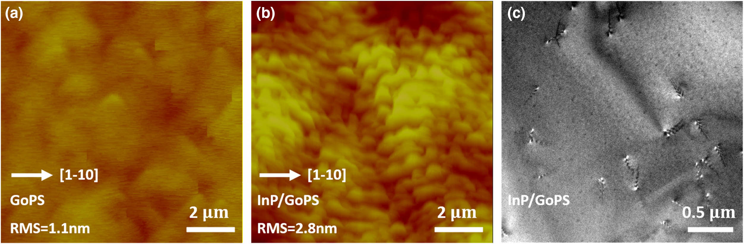
Semiconductor lasers directly grown on silicon offer great potential as critical components in high-volume, low-cost integrated silicon photonics circuits. Although InAs/InP quantum dash (QDash) lasers on native InP substrate emitting at 1.5 μm (C-band) have demonstrated notable performance, the growth of InAs/InP QDash lasers on silicon remains undeveloped because of the 8% lattice mismatch between InP and silicon. Here we report advances of growth techniques leading to the first C-band room-temperature continuous-wave electrically pumped QDash lasers on CMOS standard (001) silicon substrates by metalorganic chemical vapor deposition. A correlation between various material characterizations and device performance is analyzed for different QDash laser structures grown on planar nominal (001) silicon. With the optimized QDash growth and improved fabrication process, the lowest threshold current density of was determined on an device on planar silicon with a single facet output power exceeding 14 mW. The device results illustrate the good material quality of the QDash lasers grown on silicon, suggesting potential applications for other active components of photonic integrated circuits, such as semiconductor optical amplifiers, modulators, and photodetectors.
Photonics Research
2020, 8(12): 12001888
1 中国科学院自适应光学重点实验室, 四川 成都 610209
2 中国科学院光电技术研究所, 四川 成都 610209
3 中国科学院大学, 北京 100049
为提升光腔衰荡高反射率测量技术的精度,提出了一种基于耦合光腔衰荡技术的高反射率测量方法。该方法在耦合光腔衰荡系统中引入衰荡腔腔内模式监测模块,以腔内运行模式为判据寻找初始腔和测试腔耦合效率一致的状态,从而实现更高的测量精度。实验结果表明:在确保腔内模式处于基横模状态时,初始腔和测试腔腔内的等效损耗降低值几乎一致;对于同一高反射率待测样片,该技术对比传统方法可实现10.0%~27.1%测量精度的提升。
测量 光腔衰荡技术 高反射率测量 耦合光腔衰荡技术 基横模
1 中国科学院光电技术研究所自适应光学重点实验室, 四川 成都 610209
2 中国科学院光电技术研究所, 四川 成都 610209
3 中国科学院大学, 北京 100049
为克服光腔衰荡高反射率测量过程中初始腔和测试腔结构转换导致的腔参数相对失调,提升调腔效率,提出一种基于衰荡腔透射光斑形态监测的调腔方法。以衰荡腔透射光斑外接矩形宽高比及光斑与其外接矩形面积的比率作为调腔依据,抑制腔参数失调导致的高阶横模激发,使初始腔和测试腔透射光斑均保持在基横模状态。实验结果显示:以宽高比和面积比作为调腔依据,不仅能够分辨不同的光斑模式,同时能有效应对模式间的特殊光斑形态(如椭圆光斑、多模跳变等)。当初始腔和测试腔光斑均调节至基横模状态时,测得的样片反射率均值最高且方均根最小。结果表明该方法有助于提高光腔衰荡高反射率测量技术的调腔效率。
测量 光腔衰荡 高反射率测量 光斑模式 调腔方法

Author Affiliations
Abstract
1 Department of Electronic and Computer Engineering, Hong Kong University of Science and Technology, Clear Water Bay, Kowloon, Hong Kong, China
2 Department of Physics and William Mong Institute of Nano Science and Technology, Hong Kong University of Science and Technology, Clear Water Bay, Kowloon, Hong Kong, China
3 e-mail: phkwong@ust.hk
4 e-mail: eekmlau@ust.hk
Efficient, scalable, bufferless, and compact III–V lasers directly grown on (001)-oriented silicon-on-insulators (SOIs) are preferred light sources in Si-photonics. In this article, we present the design and operation of III–V telecom nanolaser arrays with integrated distributed Bragg reflectors (DBRs) epitaxially grown on industry-standard (001) SOI wafers. We simulated the mirror reflectance of different guided modes under various mirror architectures, and accordingly devised nanoscale DBR gratings to support high reflectivity around 1500 nm for the doughnut-shaped mode. Building from InP/InGaAs nanoridges grown on SOI, we fabricated subwavelength DBR mirrors at both ends of the nanoridge laser cavities and thus demonstrated room-temperature low-threshold InP/InGaAs nanolasers with a cross-section and a 20 μm effective cavity length. The direct growth of these bufferless nanoscale III–V light emitters on Si-photonics standard (001) SOI wafers opens future options of fully integrated Si-based nanophotonic integrated circuits in the telecom wavelength regime.
Photonics Research
2019, 7(9): 09001081
中北大学,电子测试技术国家重点实验室,山西 太原 030051
研究了锥束螺旋Katsevich和FDK重建算法,并对这两种算法进行比较。实验结果表明: 当投影数据没有噪声的时候,FDK算法和Katsevich算法均能取得较好的效果,当对实际物体进行重建的时候,投影数据含有噪声, Katsevich算法需要对投影数据求导,而它对投影数据的噪声较敏感,重建质量有所下降。
螺旋CT 图像重建 FDK算法 Katsevich算法 spiral CT image reconstruction FDK algorithm Katsevich algorithm
1 首都师范大学化学系,北京 100037
2 北京市疾病预防控制中心,北京 100013
尝试用微生物传感器、电位型酶传感和电流型酶传感器测定牛奶中残留青霉素,摸索经济、高效的测量方法,筛选出可实用的传感器.
生物电化学传感器 青霉素残留 纳米金胶 electrochemical biosensors trace penicillin nano Au colloid


